Intel Foundry Poised for Major Industry Commitments Amid Advanced Node Progress
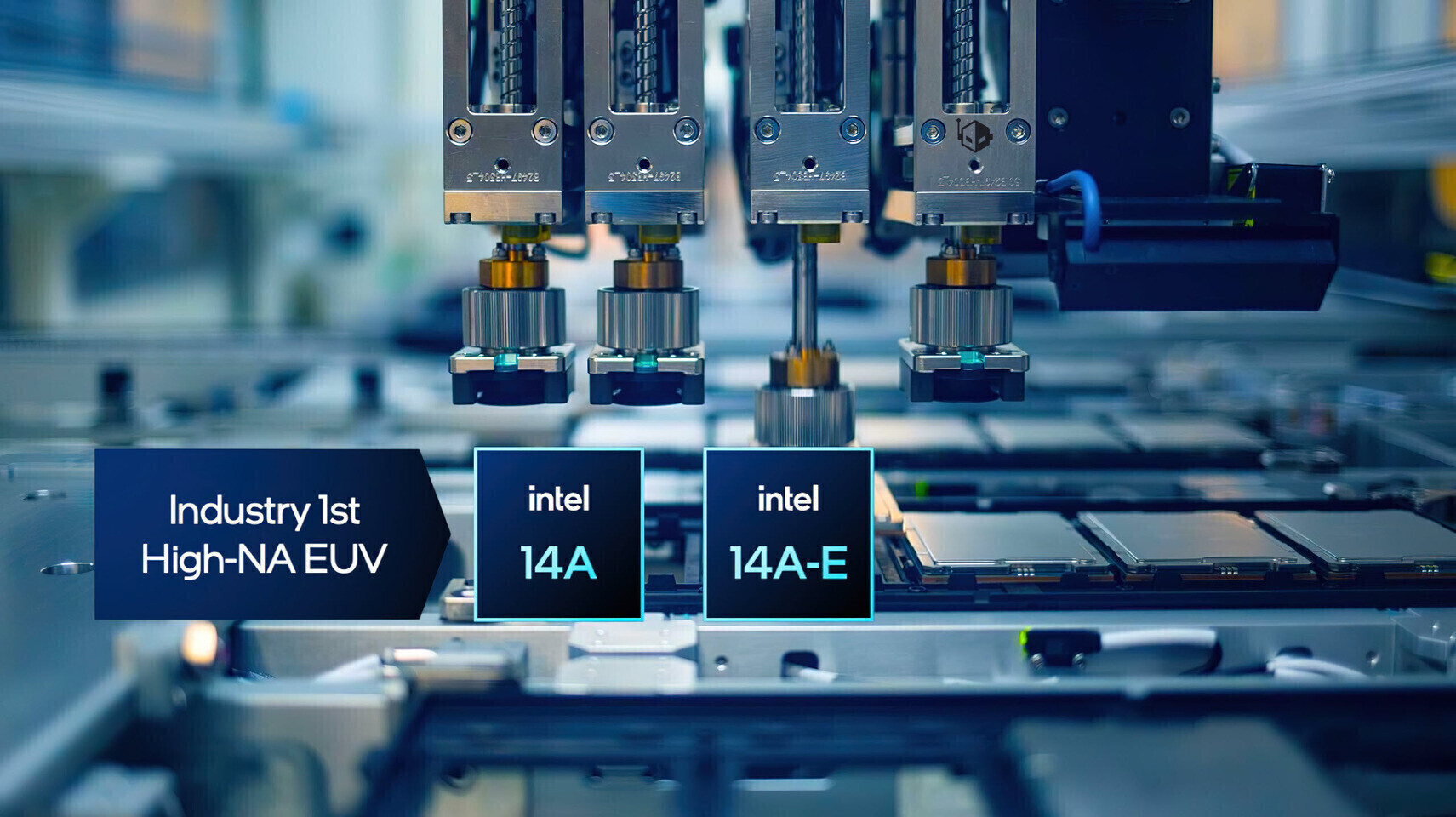
Intel Foundry is rapidly gaining momentum in the semiconductor industry, with several of the world’s largest technology companies reportedly preparing to announce new foundry partnerships this fall. According to recent analysis from UBS Group, Intel Foundry is on the verge of securing a wave of new contracts, driven in part by the release of version 1.0 of its 14A node process design kit (PDK).
Industry Giants Eye Intel’s Advanced Manufacturing Nodes
There is growing speculation that leading companies such as Apple, AMD, NVIDIA, Google, and Broadcom are evaluating Intel’s silicon manufacturing capabilities. These companies are considering Intel’s advanced process nodes, including 18A, 18A-P, 18A-PT, and the forthcoming 14A node, for their next-generation products. Notably, Apple is rumored to be planning production of some M-Series “Apple Silicon” laptop processors in 2027 using Intel’s 18A-P node. Google is also reportedly interested in leveraging Intel’s EMIB and Foveros 3D advanced packaging technologies for future TPU designs.
Intel Foundry’s Competitive Position Against TSMC
While companies routinely assess the latest process nodes from various foundries, TSMC has traditionally been the preferred choice due to its proven reliability, high-volume manufacturing capacity, and advanced packaging solutions. TSMC’s technologies have enabled the mass production of high-performance, energy-efficient chips for a wide range of applications.
However, Intel Foundry has made significant investments in both technology and logistics to attract external clients. UBS anticipates that these efforts will culminate in multiple high-profile foundry commitments being announced in the coming months. Last year, it was reported that Apple was waiting for Intel to release the 18A-P PDK version 1.0 or 1.1, scheduled for the first and second quarters of 2026, respectively. As the industry awaits further confirmation, UBS expects that Apple has moved forward with its plans.
Advanced Packaging: A Key Differentiator for Intel
Beyond silicon manufacturing, Intel Foundry’s advanced packaging technologies represent a significant opportunity for differentiation. Intel offers a suite of packaging solutions, including EMIB, EMIB-T, and EMIB-M, enabling the integration of 2D, 2.5D, and 3D chiplet architectures. These technologies allow for the stacking of multiple chiplets and the integration of high-bandwidth memory (HBM) modules within a single package. Intel has demonstrated the capability to incorporate up to 47 tiles in a single package and is exploring multi-kilowatt solutions for future high-performance applications.
In contrast, TSMC’s leading packaging technology, CoWoS, has reportedly encountered challenges when handling four reticle-sized dies, leading to production issues for some clients, including NVIDIA. This has further highlighted the importance of robust and scalable advanced packaging solutions in the semiconductor industry.
As Intel Foundry continues to advance its process nodes and packaging technologies, the industry is closely watching for official announcements from major technology companies. The coming months are expected to be pivotal for Intel’s position in the global foundry market.